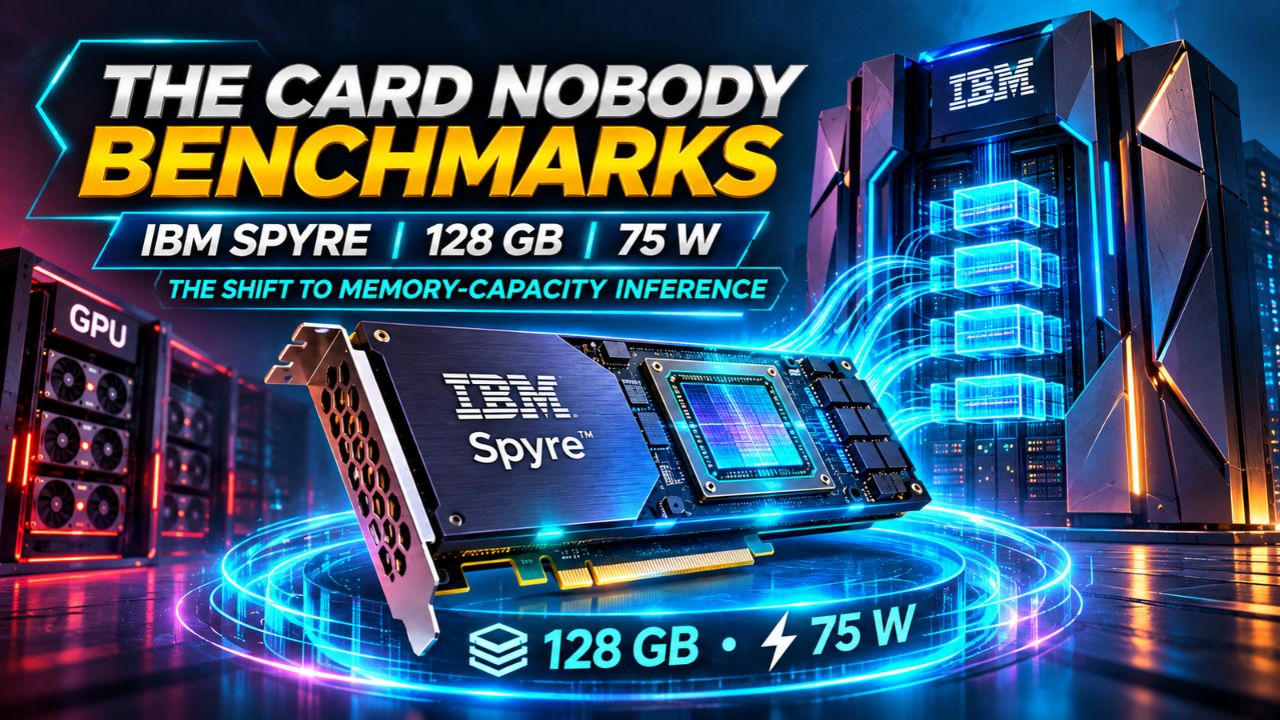
IBM is shipping an accelerator with 128 GB of memory, more than 300 TOPS, and a 75 watt power envelope, and it does not appear in a single competitive benchmark chart you have looked at this year.
It is not secret. It has been generally available since October 28, 2025, it runs inside IBM z17 mainframes and LinuxONE 5 systems, and it reached Power11 servers in early December. It is missing because every chart answers a different question, and Spyre is not trying to answer it.
The thesis is blunt. Inference is now won on memory capacity per watt, not floating point throughput per dollar, and the only vendor that shipped that trade as a product did it inside a mainframe. Spyre is not a faster GPU. It is a different bet, and the bet is checkable.
THE SPEC SHEET IS THE ARGUMENT
IBM Research published the silicon at ISSCC in February 2026, and the disclosure beats the marketing page.
The chip is 32 active accelerator cores plus two spares for yield, built in a standard 5nm CMOS process, 25.6 billion transistors, on a single slot PCIe Gen5 x16 card. Each core is split into two corelets that share one 2 MB LX scratchpad. Each corelet carries an 8 by 8 systolic array of 64 low precision math engines running fp16, fp8, int8 and int4, plus 1D vector units that keep fp32 for activations that cannot survive lower precision. There is no shared cache anywhere on the die.
The memory subsystem is the interesting part. Sixteen LPDDR5 channels at 6.4 Gbps deliver 204 GB per second peak to the cores, fed by eight dual channel LPDDR5 modules, and a bi-directional ring moves 128 bytes per cycle per direction. A card holds up to 128 GB, and eight cards in a local group reach 1 TB.
Then there is the number that decides whether your model runs. Each core can address at most 256 MB of contiguous device memory. That is a hardware limit on the addressable range, separate from the 2 MB scratchpad. It is the spec that dictates tiling strategy, kernel shape, and which models fit without heroic engineering.
The card fits a single PCIe slot budget with no auxiliary power connector, and IBM split the supply into 0.55 volt and 0.75 volt domains under a dual loop controller.
One pedantic note on the TOPS figure, because hardware reviewers will ask. IBM publishes 300+ TOPS per card and never names the precision it was measured at. An unqualified TOPS number is conventionally an 8 bit integer peak, so read 300 as a low precision integer ceiling, not fp16.
So treat 300 TOPS as a marketing number. The engineering numbers are 204 GB per second, 128 GB, 256 MB per core, and 75 watts.
WHY MEMORY-BOUND INFERENCE CHANGES THE MATH
Training is compute bound. Token generation is not. At batch size one, every generated token forces a read of the weights, so the ceiling on your token rate is memory bandwidth divided by the bytes you touch per token. That is the whole reason quantization became a research field, and it is the reason a card that wins on capacity can still lose on speed.
I ran the arithmetic, using IBM's disclosed figures and NVIDIA's published H100 numbers.
Capacity per watt: 128 GB over 75 watts is 1.71 GB per watt. H100 SXM is 80 GB over up to 700 watts, which is 0.11 GB per watt. Spyre carries about fifteen times the memory per watt.
Bandwidth per watt: 204 GB per second over 75 watts is 2.72. H100 SXM at 3.35 TB per second over 700 watts is 4.79. Spyre is 0.57 times the bandwidth per watt, so it loses this one.
Peak math per watt: 300 TOPS over 75 watts is 4.0. H100 at 3,958 dense FP8 teraFLOPS over 700 watts is 5.65. Spyre loses this one too, at 0.71 times.
That is the honest version, and almost nobody writes it. Spyre wins capacity per watt by fifteen times and nothing else, and that one axis decides whether your workload is a fit problem or a speed problem.
Here is the decision rule I use, and it is mine rather than IBM's. Compute the working set first: weights in serving precision plus KV cache at real peak concurrency and context length. Under 80 GB, a single H100 wins on latency and throughput both, and Spyre never enters the conversation. Between 80 GB and 1 TB, you shard across GPUs and make interconnect bandwidth the new constraint, or you shard across 128 GB cards that draw 75 watts each. Above that, the question stops being about speed at all.
Now look at a pattern with nothing to do with IBM. A lawyer rebuilt eight 2018 era V100 GPUs into a server running about 80 percent of DeepSeek V4.1 Flash's work at 4 bit NVFP4, at 524K context, with 1 TB of RAM and an RTX 3090 hosting the draft model. Tom's Hardware reported it. Throughput fell from a 160 to 215 tokens per second range down to 150 to 180 when he moved that work up from 2 bit to 4 bit, and he took the trade. Capacity first, and every failure catalogued in "KV Cache Memory Safety: The 37 Bugs Your GPU Sanitizer Cannot See in vLLM and SGLang" lives inside that capacity budget.
THE TILING TAX NOBODY MENTIONS
Everything above is a purchase argument. This section is the bill.

There is no hardware managed cache on Spyre. Nothing moves into scratchpad unless the compiler emitted the instruction, and nothing is divided across the 32 cores unless the compiler decided it, because the cores run as a static dataflow machine. Data moves in 128 byte sticks, or 64 fp16 values, and a kernel cannot address one element on its own.
The compiler work that follows is not a footnote. It is the product.
IBM's writeup of the torch-spyre compiler gives the cleanest example. A matmul with an 8192 by 32768 fp16 input needs 512 MB for that input alone, double the per core limit, so before anything runs the planner commits a two way split along the reduction dimension, then a sixteen way split along the output dimension. On a GPU you load the tile and go. Here the split is a compile time decision that shapes every kernel downstream.
This is also why IBM threw away its first attempt. The original compiler, called sendnn, was 273,000 lines of C++ and Python across 6,170 functions. The Inductor based replacement is 38,600 lines of Python across 1,878 functions, roughly seven times smaller, and the comparison is not apples to apples because the new code leans on PyTorch's machinery. The line count is not the finding. Maintenance friction is: code built on PyTorch's compiler inherits PyTorch's fixes and leaves the hard bugs with an outside project, not a vendor re-teaching a private stack.
The measured wins are real and they are measured against IBM's own previous compiler, not against an H100. Layout and tiling choices cut matmul kernel time by 29 to 69 percent across batch sizes and shapes. Scratchpad aware scheduling cut median softmax kernel time from 32.51 to 23.67 microseconds. A fused MLP kernel lifted core utilization from roughly two thirds to about 80 percent and cut kernel time around 17 percent. A core to core relayout replaced an 80 microsecond device memory round trip with a 1.1 microsecond on chip shuffle. On Granite 3.3 8B at batch 1 and sequence length 1024, moving graph construction off the launch path made prefill 1.7 times and decode 2.4 times faster.
What IBM has not published is a tokens per second comparison against a GPU on a named model. I looked. That absence is a finding, and it is why the card has no row in your chart.
One more tax, and this one is on you. Precision choices change how much of the 128 GB a model occupies, so the per layer decisions in "Your Quantization Is Wrong: Per-Layer Precision Cuts Inference Energy 23%" stop being an optimization and become a capacity plan. Every layer left at 8 bit costs memory and speed at once.
WHERE IT ACTUALLY RUNS
Production deployments, not pilots. A z17 or LinuxONE 5 system clusters up to 48 cards. A Power11 system takes up to 16. Forty eight cards is 6.1 TB of accelerator memory drawing 3.6 kilowatts. The same capacity in HBM would be roughly 77 H100 SXM cards at about 54 kilowatts.
Spyre exists where the data cannot move. Fraud scoring inside the payment path, claims triage, an assistant reading account history that may not leave the platform, many models serving many tenants with logical isolation on one footprint. IBM's framing is multi model inference next to the transaction, and the architecture supports it: capacity for every model a bank runs at once, power low enough to sit beside a mainframe, and an address space that keeps workloads apart.
Call it the sovereign inference play, not a datacenter disruptor. The buyer is a platform team that already owns the iron and has a compliance officer in the room. And placement still beats weights, as "Stop Tuning Weights: How Session-Affinity Routing Cut Time to First Token 85 Percent" argued: which card a session lands on sets the bill.
WHAT TO DO TODAY
- Compute tokens per watt for your three most common workloads, using 204 GB per second as the ceiling and your real weight bytes per token.
- Compute your working set, weights plus KV cache at peak concurrency, and write the number down. That number, not the model name, decides which side of 80 GB you are on.
- Check whether your serving stack can express explicit tiling and scratchpad residency, or whether it assumes a flat HBM pool with a hardware cache under it. If it assumes the pool, budget engineering time before you budget cards.
- Read the torch-spyre docs before you benchmark anything. Stick alignment, the per core limit, and compile time work division shape every result you get.
- If you run on prem for compliance, put Spyre on the shortlist and price it against per token cost at real batch size, not at peak throughput.
THE UNCOMFORTABLE QUESTION
You have been sizing inference fleets by FLOPs for three years, and the card that tries a different trade loses on FLOPs per watt, loses on bandwidth per watt, and wins on capacity per watt by fifteen times. If that is the axis your next refresh is actually constrained by, then your benchmarks have been measuring the price of a resource you were not short of.
Get More Articles Like This
Getting your AI agent setup right is just the start. I'm documenting every mistake, fix, and lesson learned as I build PhantomByte.
Subscribe to receive updates when we publish new content. No spam, just real lessons from the trenches.
Build Real AI Infrastructure
PhantomByte teaches you to build real AI infrastructure yourself: local AI stacks, autonomous agents, multi-agent orchestration, web scraping, and custom tools. Step-by-step PDF tutorials you download, follow, and deploy. No subscriptions. No fluff. Just skills that ship.