
OpenAI used its own models to help design its Jalapeno inference chip and hit tape-out in roughly nine months. That number should stop you cold. A conventional ASIC program burns years and hundreds of millions of dollars before it ever sees first silicon. Nine months is not an improvement on that timeline. It is a different category of speed.
Here is the thesis, stated bluntly. The chip design workflow, the slowest and most expensive engineering discipline in technology, is now the newest surface for AI acceleration. I covered who builds the chips in field note 153, "The GPU Era Is Not Ending. It Is Fragmenting." This note covers what designs them. The answer is changing faster than most compute roadmaps are priced for.
If you are an engineer or an infrastructure lead, this is not a story about a single company's chip. It is a story about the cost curve of every accelerator you will buy for the next five years. When the design cycle compresses, the price of custom silicon falls, and the economics of your whole stack shift underneath you. That is what this note is really about.
THE NINE-MONTH TAPE-OUT
Let me define the terms before we go further, because the stakes only land if you know what the words mean. A foundry is a factory that manufactures chips for other companies. An ASIC, an application-specific integrated circuit, is a chip built for one job rather than a general-purpose processor. Tape-out is the moment a chip design is finalized and sent to the foundry for manufacturing. That last one is the number that matters here.
OpenAI's ASIC program runs on Broadcom design services and TSMC wafer processing. Its first inference accelerator, Jalapeno, was introduced in under 18 months. The AI-assisted tape-out came in roughly nine. The design cycle, not the fab, has historically been the long pole in custom silicon. You can wait on a foundry's capacity, but the real drag has always been the years of verification, simulation, and iteration that happen before a design is ever ready to tape out. That is the part AI just compressed.
Nine months is an anomaly because the design cycle is where custom silicon has always bled time and money. A team of hundreds of engineers spends years placing cells, routing signals, running timing closure, and verifying that the thing will actually work when it comes back from the fab. AI does not replace that whole pipeline. It collapses the parts of it that are pattern recognition and search, the human iteration loop where a design goes through thousands of small corrections before it is ready. That is exactly the kind of work a model is good at, and it is exactly the kind of work that used to consume years of engineer time. The distinction matters because it tells you where the ceiling is. AI is not inventing new physics. It is not making transistors smaller or electrons faster. The more the loop compresses, the more of the discipline becomes a model problem rather than a staffing problem, and the slowest discipline in tech just got a speedup at the exact point where the industry was bottlenecked.
THE TWO-WAY DEPENDENCY
Now look at the loop forming between Qualcomm and Amazon. AWS uses Qualcomm silicon for inference. Qualcomm uses AWS Bedrock to help design its own chips. Read that twice, because it is the whole story in two sentences. The company that runs AI is buying chips from the company that uses AI to design those chips.
I am going to name this framework so it is citable, and I will use the same name every time: the Design-Loop Feedback. When AI compresses the design cycle of the hardware that runs AI, every generation of models gets cheaper chips faster, and every generation of chips makes designing the next one faster. That loop is the story. It is not any single press release. It is a self-reinforcing cycle where the tool and the hardware it runs on accelerate each other.
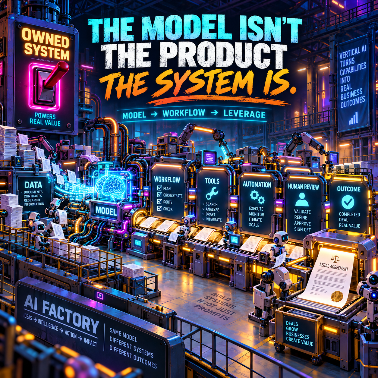
This is not a curiosity. It is the mechanism that decides who wins the next decade of compute. The companies that close the loop, that let their models design the silicon that runs their models, get a compounding advantage. The companies that treat chip design as a walled-off discipline staffed only by humans are going to watch that gap widen every single quarter.
The Qualcomm-Amazon deal is the cleanest example of the loop because it is two companies on opposite sides of the same cycle. Amazon runs its own Trainium and Inferentia hardware programs, so it is not a stranger to custom silicon. But it is still buying Qualcomm parts for inference, and Qualcomm is still using Amazon's AI to design those parts. Neither company is betting the whole stack on one side. They are both hedging across the loop, and that is the rational move when the loop is accelerating.
WHY SAMSUNG RUNS ITS MODELS ON-PREM
Samsung is deploying on-premises Mistral Large models inside its fabrication workflows. That sentence matters more than it looks like. Process recipes and yield data are the most guarded trade secrets in the entire semiconductor supply chain. They are the accumulated knowledge of how to actually make chips at scale, and they are worth more than any single product. That is why the frontier AI cannot touch them from a cloud API. You do not ship your crown jewels to a third party's server.
This is the sovereign-AI pattern applied to manufacturing. The same on-prem logic I have covered for national AI stacks applies inside a single fab. For anyone new to the term, on-premises means the model runs on machines you control, and the data never leaves your network. The model comes to the data. The data does not go to the model.
That distinction is the entire point. Samsung is not worried about the model's capability. It is worried about where the data lives. The moment a process recipe or a yield curve crosses a network boundary, it is no longer fully yours. Running the model on-prem keeps the knowledge inside the walls. This is the template for anyone running models near trade-secret data, and it is not optional anymore.
The same logic that pushes a national AI stack onto sovereign infrastructure pushes a fab onto on-prem models. The data is the asset, and the asset does not leave the perimeter. Samsung is not making a philosophical point about open weights. It is making a security decision about its most valuable intellectual property. Every company that runs models near process, yield, or pricing data should be making the same decision, and most of them are not.
THE PHYSICAL WALL STILL STANDS
Now the balance, because the hype deserves a counterweight. Executives at Goldman's Communacopia conference said power, wafers, and memory remain the physical constraints on AI growth. Those are not software problems. You cannot prompt your way to more electricity, more silicon, or more memory bandwidth.
TSMC is fully booked by AMD and Nvidia. That is why OpenAI is courting Samsung Foundry as a second source. Broadcom's AI chip revenue is up 221%, which signals real custom ASIC demand, but it does not signal unlimited supply. Demand and supply are different things, and the gap between them is the constraint.
Design cycles compress. Physics does not. AI can shrink the drawing board, but it cannot mint more wafers. The speedup in design is real and it is compounding, but it operates inside a physical envelope that is not getting any bigger. Anyone who reads the nine-month tape-out and concludes that the silicon shortage is over is reading the wrong chart.
This is the part of the story that keeps the whole thing honest. The design loop is a genuine acceleration, but it runs on top of a supply chain that is still constrained by wafers, power, and memory. OpenAI is courting Samsung Foundry precisely because TSMC cannot take more work. Broadcom's 221% revenue jump is demand, not capacity. The loop makes the drawing board faster. It does not make the factory bigger.
WHAT TO DO TODAY
- Audit your compute roadmap assuming custom silicon design cycles are compressing from years toward months. Your next contract negotiation should price that in, because the cost of custom silicon is about to fall faster than your vendor wants to admit.
- If you run models near trade-secret data, process, yield, or pricing, plan an on-prem or private deployment now. The Samsung-Mistral pattern is the template. Do not wait for a breach to justify the architecture.
- Track the Design-Loop Feedback when you forecast inference costs. Faster chip design means cheaper tokens per generation, independent of model quality. That is a cost curve you can plan around, and it is separate from the model-competition curve.
- Watch the second-source foundry story, Samsung joining TSMC for OpenAI silicon. Double-sourcing means supply, but it also means your accelerator roadmap can survive one foundry's booking crunch. Build that redundancy into your own planning.
THE UNCOMFORTABLE QUESTION
If a model can tape out a chip in nine months, what exactly is your engineering moat? And if your answer is experience, how long does that answer survive companies whose models get better every time they design a chip? The loop does not wait for you to catch up. It compounds on its own schedule.
Get More Articles Like This
Getting your AI infrastructure right is just the start. I'm documenting every optimization, cost lesson, and architectural insight as I build PhantomByte.
Subscribe to receive updates when we publish new content. No spam, just real lessons from the trenches.
Build Real AI Infrastructure
PhantomByte teaches you to build real AI infrastructure yourself: local AI stacks, autonomous agents, multi-agent orchestration, web scraping, and custom tools. Step-by-step PDF tutorials you download, follow, and deploy. No subscriptions. No fluff. Just skills that ship.